Research Projects
Our research extends conventional nanofabrication techniques beyond the state of the art and adapts them to address questions in cellular and molecular biophysics, and, conversely, to exploit the unique properties of biomolecules in order to build new types of electronically functional devices. This work is highly interdisciplinary as well as highly collaborative and has involved partners in several departments at Columbia University and other universities and research centers.
Nanofabrication
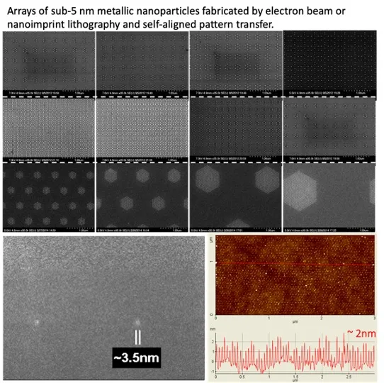
Ours is one of the leading groups in the world at “making things small.” Using a variety of techniques, ranging from electron beam and nanoimprint lithography, innovative pattern transfer methods, thin film deposition and processing, self-assembly and directed self-assembly, we routinely create structures with dimensions as small as 2 nm, which is approximately the width of a DNA molecule. We apply these techniques to a variety of studies, ranging from advanced nanoelectronics to biomolecular and cellular interactions.
Nanoelectronics
The semiconductor industry has, for years, been seeking alternatives to traditional silicon scaling, which is the systematic reduction of transistor size that has fueled the incredible growth in computational speed and power, but which faces ultimate physical limits in the coming decade(s). New materials, such as semiconductor nanowires and carbon nanotubes, have outstanding electronic properties and have shown great promise for future applications, yet they face some significant challenges to implementation. Using our nanofabrication tools, we explore new ways of addressing some of these issues, particularly for carbon nanotubes.
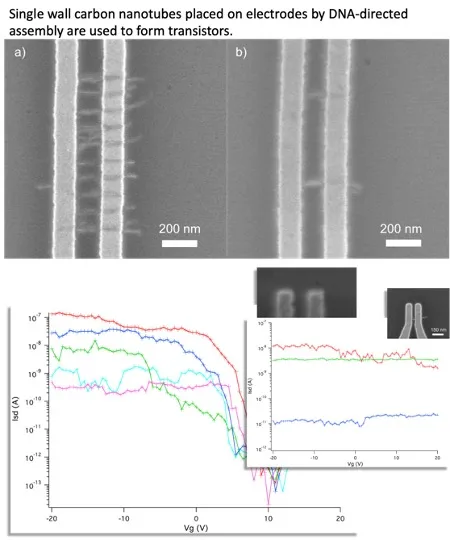
- Biological and Biologically Inspired Assembly of Functional Nanostructures – As an example, we have been exploring new ways of forming carbon nanotube devices and circuits by organizing them on surfaces using a combination of nanolithgraphic patterning and DNA assembly.
-
Bioelectronics – Biomolecules possess a variety of unique properties that have attracted interest for their potential use as electronic materials. DNA, in particular, has been the subject of intense research for several decades, and there have been a range of claims about DNA’s ability to conduct electricity, with reports over the years that DNA is (a) metallic; (b) insulating; (c) semiconducting; and (d) superconducting. These conflicting reports are primarily a reflection of the difficulties encountered in measuring the charge transport properties of single molecules. Fortunately, there has been much progress in this area in recent years, and using techniques that we have developed, we are improving our ability to determine the true electronic properties of DNA.
Beyond creating platforms for measuring DNA conductance, we are also exploring some DNA variants that look very promising as molecular wires. Even more intriguing is the potential of these wires to organize themselves into complex topologies that might (someday) form the basis for a new type of signal processing.
Quantum Nanosystems
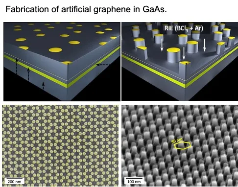
- Artificial graphene
- Deterministic placement of nitrogen vacancies in diamond
Biophysical Studies
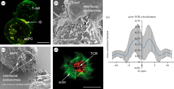
Physical factors in the environment of a cell regulate cell function and behavior and are involved in the formation and maintenance of tissue. We work with biologists and biomedical engineers to develop new tools that enable us to gain unique insight into how cells sense force, stiffness and geometry. Developing an understanding of how these physical factors affect cell function and behavior can form the foundation for new types of diagnostic and therapeutic treatments of various diseases and can guide the rational design of tissue scaffolds that can optimize healing while minimizing scarring.
- Cellular Mechanostransduction
- Platforms for Single-Molecule Studies